Diamond Information

Optical Measurements (Metrology) of Diamond

Due to the inherent transparency of diamond across a wide wavelength range, optical methods of characterization have long been the go-to methods for characterizing inclusions, impurities, and color-causing defects. Except for diamond window applications, it is usually these features that make the diamond most interesting or valuable.

Physical Properties of Diamond

Diamond is the hardest of all natural materials.  The hardness of any given material is usually determined by pressing a carefully shaped indenter onto a surface under a load, resulting in a permanent plastic deformation.  Read more…

Optical Properties of Diamond

Diamond is transparent from the UV (225 nm) to the far infrared. Only minor absorption bands exist resulting from two-phonon absorption between 2.5 and 6.5 µm. This makes diamond an ideal material for multispectral optical Read more…

Thermal Properties of Diamond

Diamond is unmatched as a thermal conductor.  It  is  informative  to  compare  the  thermal  conductivity  of diamond to that of other materials with which  it may be used or with which  it may compete. Polycrystalline Read more…

Electronic Properties of Diamond

Diamond’s potential as an electronic material has become legendary by virtue of its wide band gap (5.5eV), high carrier mobility, breakdown field, saturation velocity, and thermal conductivity.  If this potential can be realized, diamond is Read more…

Our Most Popular Products

Check out the Custom Quote Request tool for other sizes and specifications.

CVD Diamond Plate 7.0 x 7.0 mm

Optical grade single crystal diamond plates

Tolerances:

  • Lateral dimensions +/-0.2mm
  • Thickness: +/-10%

Custom Quote Request

A diamond product tailored to your application.

CVD Diamond Plate 9.0 x 9.0 mm

Optical grade single crystal diamond plates

Tolerances:

  • Lateral dimensions +/-0.2mm
  • Thickness: +/- 10%

HPHT Diamond Plate

1mm thick diamond plate, (100) orientation on large faces, high nitrogen content, grown via a high-pressure, high-temperature (HPHT) process.

Evolve Diamonds Is Making A Splash

Material Research Society

Upcoming Conference Appearance: Dec 2024

Oral Contributor - Material Research Society Fall Meeting

Laser-induced graphitization interior to bulk diamond forming monolithic electronic structures.

UMass Core Facility Voucher Awardee: Sept 2024

UMass Core Facility Voucher Awardee: Sept 2024

Voucher award grants discounted access to 90 core equipment facilities at 5 University of Massachusetts campuses.

NEMC Hub logo

Evolve Diamonds Joins Northeast Microelectronics Coalition: July 2024

The Northeast Microelectronics Coalition (NEMC) Hub is a network of 200+ organizations, including commercial and defense companies, leading academic institutions, federally funded R&D centers (FFRDCs), and startups concentrated in eight Northeast states. Established in 2023 and funded through the CHIPS and Science Act, the NEMC Hub is one of eight regional Microelectronics Commons Hubs acting on a shared mission to expand the nation’s global leadership in microelectronics and accelerate domestic semiconductor prototyping.

Defense Advanced Research Projects Agency logo

DARPA R&D Grant Awardee: June 2023

Large Area Device-Quality DIamond Substrates (LADDIS)

LADDIS seeks to develop techniques for substrates for diamond semiconductors with diameters larger than 50 millimeters, dislocation density below 103 square millimeters, surface roughness below 0.2 nanometers, and good electrical, thermal, and mechanical properties.

Conference Appearance: Dec 2019

Conference Appearance: Dec 2019

Invited Speaker - Material Research Society Fall Meeting

Rapid Growth of High-Quality Single
Crystal Diamond by a Toroidal Plasma
Process: New Domains Enabled by Computational Fluid Dynamic Modeling

Conference Appearance : Jan 2019

Conference Appearance : Jan 2019

Diamond D-Day International Workshop - Bristol, UK

Reporting on the
*Low-strain diamond epitaxy on a high strain substrate
*Growth rates of 160 um/hr of optical grade material.
*Low-temperature (650C) polycrystal growth rates up to 6.2um/hr

Physica Status Solidi (a) Cover: Nov 2018

Physica Status Solidi (a) Cover: Nov 2018

Diamond Power Field Effect Transistors

Diamond's properties (highest thermal conductivity, high hole & electron mobilities, & high electric breakdown field) predict that diamond field‐effect transistors (FETs) will have superior high‐power high‐frequency performance over FETs formed in other semiconductors. This article reviews the state of the art for FET and substrate development.

USA Patent Issued: June 2018

USA Patent Issued: June 2018

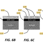
US9,991,113: Systems and Methods for Fabricating Single-Crystalline Diamond Membranes

A buffer layer is employed to fabricate diamond membranes and allow reuse of diamond substrates. In this approach, diamond membranes are fabricated on the buffer layer, which in turn is disposed on a diamond substrate that is lattice-matched to the diamond membrane.

Diamond & Related Materials: Mar 2018

Diamond & Related Materials: Mar 2018

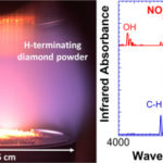
Chemical and semiconducting properties of NO2-activated H-terminated diamond

After NO2 exposure of H-terminated diamond, used for field effect diamond transistors, no NO2– is present on the diamond surface, but instead NO3–.
Surface H and NO3– concentrations and surface conductance are stable in dry N2.

Why work with us?

Responsive

Next-day shipment of in-stock products |
Custom quotes within 48 hours

Quality

Quality assurance reporting with every shipment |
Custom specifications welcome

Support

USA-based technical support |
Consulting services available for in-depth application engineering

Experience

15 years of CVD diamond growth and development |
Regular appearances at international diamond conferences.

Security

Security Clearance clearable |
No foreign ownership

info@EvolveDiamonds.com
Call +1 (978) 4 DIA CVD
        +1 (978) 434-2283
LinkedIn